
Welcome to
the Forum
Engage innovators and practitioners on the edge of technology advancement.









.webp)
OpsRamp Shows Unified IT Operations for Fast Incident Management
OpsRamp, an HPE company, claimed their turn in the spotlight during Cloud Field Day to demo their impressive unified and AI-powered IT operations management platform. The software-as-a-service solution addresses one of the most persistent challenges in modern IT operations: the complexity of managing multiple environments, tools, and data sources scattered across on-premises and cloud infrastructures.
OpsRamp’s foundation is based on a three-pronged strategy:
First, the platform provides unified observability by consolidating all data from applications, servers, network devices, and cloud environments into a single tool.
Second, it offers AI-powered analytics to help operators understand what’s happening across their infrastructure so they can prevent and solve problems.
Third, it includes intelligent automation for corrective actions when issues are detected, potentially reducing resolution times from days to hours.
The architecture’s flexibility stood out as particularly practical. OpsRamp offers both agent-based and agentless monitoring approaches, with their lightweight Go-based agent consuming minimal resources. The platform integrates with over 3,000 third-party tools and can act as a “monitor of monitors,” ingesting alerts from existing solutions via webhooks. Once the alerts are ingested, OpsRamp can apply its AI-powered analytics to do alert correlation. This coexistence capability addresses the reality that most organizations can’t just replace their entire monitoring stack overnight.
From a business perspective, the subscription-based licensing model seems straightforward, charging per monitored resource (e.g., a server, network device, wireless access point, or even a public cloud resource) with different ratios for different device types: a server counts as one resource, while four wireless access points count as one resource. The platform includes up to 50 metric series per resource with 12-month data retention for metrics by default.
What impressed me during the live demonstration was the platform’s alert correlation capabilities. The team showed how OpsRamp’s machine learning can identify cascading failures—like when a single network switch port failure triggers multiple alerts across virtualization layers, databases, and applications. Instead of overwhelming operators with many individual alerts that require manual correlation, the platform creates what OpsRamp calls “inference alerts” that group related incidents together and identify the probable root cause.
The TechArena Take – Transformative IT Incident Management
OpsRamp represents a holistic response to the persistent problem of IT operations complexity. The presenters made a compelling case for moving beyond the siloed tool approach where organizations may have separate platforms for network, storage, compute, database, and cloud monitoring. The combination of comprehensive observability, intelligent correlation, and governed automation creates a compelling value proposition. The platform’s ability to work alongside existing tools rather than requiring wholesale replacement makes it particularly attractive for enterprise environments with significant legacy investments.
The alert correlation capabilities using machine learning could genuinely transform how operations teams handle incidents. For organizations struggling with alert fatigue and the operational overhead of maintaining multiple monitoring silos and correlating the data to trouble-shoot issues, OpsRamp offers a remarkable solution.
MinIO Redefines Object Storage Architecture for Exabyte Scale
MinIO brought Cloud Field Day 23 to a strong finish with a presentation on their flagship enterprise offering, AIStor, highlighting the critical shift toward object-native storage for AI and analytics workloads.
Object storage is critical to today’s AI and analytics landscape. Every major large language model (LLM) was built using object storage, and all data lakehouse analytics tools have become object-native by design. This isn’t surprising since cloud providers like AWS S3 are inherently object-native, but it presents challenges for on-premises deployments.
The core problem MinIO addresses is the architectural limitations of traditional retrofit object gateway solutions. These systems stack multiple layers, including a gateway layer for translation, a metadata database, a storage area network or network attached storage (SAN/NAS) backend, and a storage network. These layers create performance bottlenecks, data consistency issues, and scale limitations.
MinIO’s AIStor takes a fundamentally different approach with a gateway-free, stateless architecture using direct-attached storage. This eliminates the translation layer and central metadata databases, instead writing metadata atomically with the actual data; a deterministic hashing approach actually avoids the need to have a central database at all. The result is guaranteed read-after-write and list-after-write consistency at massive scale, something impossible with traditional approaches.
A key differentiator for AIStor is its truly software-defined nature, meaning it can run on any industry-standard hardware. Unlike storage solutions that require specific appliances, MinIO works across the spectrum from small deployments on a Raspberry Pi to massive 1,000+ node clusters. The company recommends minimum system requirements for serious production environments, and recommends NVMe drives over hard drives, but runs off any industry off-the-shelf hardware.
Real-world deployments demonstrate AIStor’s capabilities. A large autonomous vehicle manufacturer runs 1.35 exabytes on AIStor, when previous platforms failed at 20 to 50 petabytes (PB). A leading cybersecurity company is running about 1.25 PB on AIStor, having repatriated data out of AWS, and the transition helped improve their gross margin around 2 to 3%. Finally, a fintech payments provider serving nearly half a billion merchants and processing billions of small files is currently running 30 PB with a plan to scale to 50; they’re meeting strict service level agreements that their previous appliance-based solution couldn’t handle.
The TechArena Take – AIStor’s Architecture Stands Out
MinIO AIStor represents a powerful solution for enterprises serious about AI and analytics at scale. The object-native architecture addresses fundamental limitations of traditional “unified” solutions, while real-world deployments prove the technology works at exabyte scale. For organizations moving beyond test environments into production AI workloads, AIStor is a smart choice for a solid foundation that can grow from petabytes to exabytes without architectural rewrites.

Qumulo Showcases Cloud Data Fabric Innovation
Qumulo’s presentation at Cloud Field Day 23 highlighted their innovative approach to unstructured data storage across hybrid cloud environments. The company, known for their advanced file system technology that enables unified global data management across data centers and clouds, has built a customer base spanning entertainment, healthcare, pharmaceuticals, and government sectors during their 13 years in business.
The core of Qumulo’s offering is their cloud data fabric, designed to unify data across any hardware platform and cloud environment. The company’s solution works with unstructured data, which is 80% of what feeds enterprise systems and includes film/video, images, telemetry, game builds, mapping/GIS, and more. By supporting data on any hardware and any cloud, it gives customers infrastructure freedom of choice and allows them to choose the configuration that is best for them.
Central to Qumulo's approach is building a strictly consistent, very correct, and very durable file system that extends authentication and authorization to surrounding systems. This ensures data is available to authorized users in its most accurate and consistent form, which is critically important for AI applications that depend on current, correct data. The system can treat distributed data pools as a single file system while maintaining local performance characteristics, addressing pain points around data gravity and geographic distribution.
I was blown away by Qumulo’s customer testimonials as their value proposition came to life. The company believes they are in 10 of the world's 10 largest video production houses, with many recent major releases having some connection to their infrastructure. In pharmaceuticals, they support 10 of the 10 largest recipients of grants from the National Institutes of Health and National Science Foundation. They also handle critical applications like wildfire modeling for Southern California firefighters and real-time crime center operations.
The TechArena Take – Innovation for Real Problem Solving
What impressed me from the talk was Qumulo’s focus on solving real operational challenges. Their cloud data fabric addresses pain points around data gravity, geographic distribution, and strict consistency across hybrid environments. The ability to treat distributed data pools as a single file system while maintaining local performance is technically impressive and practically valuable.
Customer stories demonstrate clear ROI, from helping mortgage underwriters improve productivity from 3 to 14 applications daily with AI processing technologies to enabling global visual effects collaboration without traditional data movement constraints. The combination of technical innovation with real-world problem-solving makes Qumulo compelling for enterprises dealing with large-scale unstructured data challenges.

HPE Greenlake Paves a Path to a Hybrid SAP ERP Future
The HPE Greenlake team and SAP team joined together at Cloud Field Day 23 to kick off proceedings on June 5, and the topic was SAP ERP. SAP HANA, first delivered in 2010, provides enterprises an in-memory database that fuels the S/4 HANA ERP solution. S/4 has had mixed results in the market, driving SAP to introduce SAP Cloud ERP, a platform as a service offering, as an alternative to on-prem packaged deployment.
The HPE team delivered a message that SAP’s evolution of this solution in this marketplace has challenged customers, requiring too much change and too rigid of solutions to get traction with the solution in market. Yet, early adopter key learnings represent a new approach to the market enabled by Greenlake. This will enable enterprises to run this solution in their own data centers (managed by HPE) and navigate end of life of the traditional ERP solution coming in 2027. The solution also provides a path to multi-tenancy and public cloud adoption.
How does this solution come together? Private cloud ERP will be delivered with SAP support. The cloud ERP provides a foundation for layering on ecosystem solutions and Joule agents to drive functions like finance, spend, supply chain HR, and customer service. The team has packaged this as software plus infrastructure management and services, cloud services, and upgrade support into one integrated solution.
Why is this important?
The collaboration provides a path to simplified adoption for enterprises, and we expect SAP and HPE are banking on this single solution to help accelerate adoption of what has been a clunky solution. The public cloud ERP is touted to be simpler to use, and integration of Joule agents are touted as productivity drivers for across the enterprise. With ecosystem solution integration, the team has provided flexibility for deploying solutions that are tuned for unique enterprise environments with a common ERP foundation. This path has a lot of value for large organizations that don’t want the complexity of managing an on-prem implementation but still want control of their most precious data within a managed private cloud.
What’s the TechArena take?
SAP is a complex and powerful solution, and kudos to the SAP team for recognizing the complexity of traditional deployment models. HPE understands enterprise-class requirements for data security and control and makes a solid partner choice for this delivery. While I would like to have heard more in the presentation on why customers benefit from this SAP RISE solution vs. competitive offerings in what still feels like a very heavy lift, there’s no question that enterprise has relied on SAP and will continue to do so with this modernized solution.

.webp)
TechArena Great Debate: Google Talks OCP LOCK and Open Standards
Amber Huffman and Jeff Andersen of Google join Allyson Klein to discuss the roadmap for OCP LOCK, post-quantum security, and how open ecosystems accelerate hardware trust and vendor adoption.

Scality Showcases Real-World Resilient Cloud Storage Solutions
Scality brought the heat at Cloud Field Day 23, telling their story through the lens of customer success. The company, which has been working in the storage software arena for the last 15 years, discussed the latest with Scality Ring. Their history started with the rise of the cloud, responding to service providers needing a storage foundation extending into enterprise on-prem cloud storage solution delivery.
With this foundation, Scality began pivoting to AI data lakes a few years ago, adding integration of security and data aggregation, feeding the initial phases of data cleaning before being utilized for AI training. They differentiate with extreme scaling, supporting 1 to 1000s of apps, 100 petabytes (PB) per failure domain, 100s of billions of objects, and more.
We walked through a number of use cases, starting with Splunk. Ben Morge walked through a case study of a US-based bank with a 30-40 PB Splunk data store across multiple sites and 1-year data retention. Ben described the configuration featuring SSD-based hot-tier data connected to Ring warm-tier backup. Data is replicated across sites tapping HPE Apollo servers. The complexities of this configuration involved mitigating migration ingest overload and unexpectedly high production GET traffic, addressed by increasing server capacity to maintain a 75 GB/GET throughput per site. The result? Tiering with this approach provided a resilient multi-site storage solution with the required retention policy.
Next up was Nick Sayer, describing a challenge tackled for CNES, a multi-PB satellite imaging storage with data retention of new imagery in hot tier for 6 months along with multi-hundred PBs of cold-tier image data. The customer had a hodgepodge of storage environments and wanted to convert multiple formats to S3 in a cost- and energy-efficient environment.
The solution? A hot/warm tier Ring across three data centers in a single namespace S3 data lake coupled with a cold-tier tape solution. Any user query seeking data on tape is prompted to restore from cold tier on a temporary basis to utilize the data before it’s returned to its tape home. The multi-site tape solution stretched Ring capabilities, requiring support across multiple public clouds and tape providers and requiring a unique API development by the Scality team to deliver the resilience required for tape solutions.
Next up was Aurelien Gelbart providing insights on a French bank deployment integrating multiple storage solutions for internal data with an aim of lower price per TB with a bill-back solution to business groups for usage. The challenge was moving over 2,000 applications’ data to be integrated into one Ring platform, including database backup, financial data, data lake, DMS, artifacts and media. The solution required rapid scale, growing from 1 to 50 PB over seven years. Scality tackled this solution with software improvements that handled this complex environment as well as architectural improvements that allowed server flexibility. The solution today supports 100 PB of storage and over 300 billion objects and 1 billion client operations per day, offering incredible scale and resiliency for the bank…all with a cost reduction of 75%, primarily driven by consolidation of systems across business groups.
The TechArena Take – Resilient and Scalable Storage
With these customers and more relying on Scality’s scale, flexibility, and engineering know-how, it’s no wonder that global brands rely on the software for storage integration. We like the way the team shared how they work with customers to solve unique challenges, speaking to the deep level of collaboration required for these large-scale deployments. We see value in how they tackle unique opportunities like tapping cold-tier tape and mitigating the complexity with collaborations and custom API development. We see no end of demand as more companies seek AI data lakes to fuel broad scale AI deployments. In other words…we expect to see more fantastic customer deployment stories from Scality in the months ahead.

Palo Alto Networks Uses AI, ML to Reimagine AI-Era Cybersecurity
DALLAS – June 4, 2025 — Several Palo Alto Networks executives took the stage for the company’s Ignite on Tour event in Dallas, delivering the clear message that complexity is the enemy of security, and AI is both the threat and the answer.
In a morning packed with insightful commentary, real-time attack simulations, and partner insights from Sabre, CDW, and others, the Palo Alto Networks team made the case for a new security architecture built from a unified, intelligent platform.
AI Is the New Oil — And Also the Fire
Kumar Ramachandran, president of network security at Palo Alto Networks, opened with a bold analogy: today’s AI inflection point mirrors the petroleum-fueled transformation of the 1900s. As in the dot-com era, he noted, companies faced a decision – lead the change or be changed by it.
Kumar described a seismic shift in the nature of cyberattacks, saying the time period between reconnaissance and impact is now greatly truncated.
“The time period has shrunk from what used to be weeks, if not multiple weeks, to a few small hours,” he said. “The much larger percentage of attacks feel like a zero-day attack.”
With attackers using LLMs for reconnaissance, phishing, and vulnerability discovery, traditional defenses are crumbling under speed and volume, he said.
Palo Alto Networks’ prescription? A fully integrated security platform that fulfills what he called the “three C’s” of modern data: complete, consistent, and correct. In a world where the average enterprise juggles 83 security tools across 30 vendors, that level of data quality isn’t achievable through manual integration.
The company outlined its three major platform pillars:
- Zero Trust Network Security: Combining firewalls, SD-WAN, and SASE into a unified stack with shared policy and AI-powered threat prevention.
- AI-Driven Security Operations (XSAIM): A unified SOC experience powered by more than 7,000 detection models and capable of reducing 19,000 alerts to 17 actionable incidents daily.
- Cloud-Native Security: Including posture management, application security, and real-time cloud detection and response.
The unifying thread is automation powered by AI – not just to detect threats, but to understand context and reduce human overhead across environments.
AI Is Transforming Work – and Creating Risk
Anupam Upadhyaya, SVP of SASE products, demonstrated how AI is both a productivity accelerant and a security nightmare. At Palo Alto Networks, internal developer productivity has increased by 20–30% thanks to AI copilots and code assistants, he said.
But these tools create new vulnerabilities. Anupam showcased AI Access Security, a tool that gives organizations visibility into which generative AI tools employees are using – including shadow AI – and how those tools are handling sensitive data. The platform allows teams to classify, tolerate, or block AI apps with contextual policy enforcement.
Also unveiled was Prisma AI Runtime Security, providing full-stack protection from agents to models to data sets. The demo showed real-time revocation of malicious model permissions and red teaming tools that simulate agentic AI attacks before they happen.
Sabre’s Story: From Chaos to Control
Scott Moser, senior vice president and CISO of Sabre Corporation, shared a compelling journey from 28 security incidents per year to near real-time remediation. After consolidating from four endpoint tools to one – Palo Alto’s XDR – Sabre reduced mean time to containment from days to hours, with 60% of alerts now fully automated.
He emphasized the importance of trust and partnership, citing Palo Alto’s support during previous incidents as the differentiator.
“They didn’t just sell us software,” he said. “They showed up.”
Live Fire: Inside a Real-Time GenAI Attack
The most riveting moment came from Unit 42’s Carl Bryant, who walked the audience through a red-teamed, AI-driven attack modeled on MITRE ATT&CK. What once took days – recon, privilege escalation, payload delivery – could now take minutes using agentic AI.
His warning to retailers was blunt: “You’re in the bullseye for the rest of the year.”
With GenAI tools being abused by threat actors in China, North Korea, Iran, and Russia, Carl emphasized that organizations need AI-powered defenses simply to survive.
The TechArena Take
Palo Alto Networks didn’t just pitch a product suite in Dallas – they delivered a clear and urgent thesis: cybersecurity must move as fast as attackers do, and the only viable response is platformization – as they call it – anchored in AI and automation.
The implication? If you’re still piecing together best-of-breed tools from a dozen vendors, you’re not solving security; you’re maintaining a jigsaw puzzle that’s missing critical pieces. From cloud runtime protection to AI access control to unified SOCs, Palo Alto is betting that convergence, not complexity, will define the next decade of enterprise security.

TechArena Fireside Chat: OnLogic Talks Edge Compute Density
Hunter Golden of OnLogic joined Allyson Klein for a candid conversation on scaling edge infrastructure, avoiding over-spec'ing, and right-sizing hardware for evolving AI workloads.
After the video check out the Edge Server Selection Checklist here.

End of an Era: Why Enterprise is Bailing En Masse from VMware
The arena of tech promises constant change, heady innovation that propels us forward, new entrants delivering solutions that were beyond imagination a few months ago, and of course, era-ending transitions when companies that were foundational pillars somehow collapse. We’ve seen and covered this last narrative as it’s played out over the last few years with Intel, the once North Star of compute platform definition. Now, a new behemoth has emerged that may be following in Intel’s unforced error footsteps – VMware.
VMware…the inventors of modern virtualization. VMware…the foundation of the private cloud. VMware…every IT manager’s best friend. That VMware.
We knew that when Broadcom acquired VMware, we’d see a transformation of the business. Hock Tan certainly carries a reputation with him of financial success and efficient operations. Many wondered how this approach, effective in hardware component delivery, would fit with v-admins. As the story has evolved, we’ve seen business decisions that have disrupted the long-held trust that enterprise IT has had in VMware for decades. Changes in licensing agreements, ramps in core-licensing minimums, and more have rolled out from new leadership, and with it a growing sense of uncertainty whether VMware can be trusted as a foundation of private cloud moving forward.
At TechArena, we’ve been watching this story evolve and wanted to check in on enterprise sentiment. We conducted a survey of IT operators at Dell Tech World, a terrific opportunity to get to the heart of what enterprises are thinking about data center computing, to see how IT organizations were viewing this landscape, and, more importantly, what they planned to do about it. What we found was eye-opening, even given our suspicions that VMware’s rock-solid hold on enterprise was wavering.
Active Migration is Happening
IT respondents reflected that migration is absolutely a priority in many organizations, with 10% of respondents having already migrated off of VMware solutions and a whopping 28% currently planning a migration. Given that 19% of respondents claimed that they weren’t VMware users, this reflects almost half of those using VMware historically within some state of migration.

Migration Signals Modernization
So what will drive IT destinations? In looking at top feature priorities for IT deployments, two items bubble to the top: 31% of respondents signaled that support for a wide selection of IT infrastructure was a top criterion, and an additional 25% tapped integration of cloud-native features as essential. While migration is very much a move from a platform, the move to what’s up next will be driven by full features that will support modern private clouds. This provides some insight into how IT organizations dislike anything that feels like lock-in and want options for modern integration of features like containers that will propel the advancement of IT operations and provide new inroads for adoption of new classes of applications like enterprise’s expected ramp of AI.

So what’s the TechArena take? As Keith Townsend recently quipped, “there’s nothing wrong with VMware”, and from a narrow view of technology capability, he’s absolutely correct. What’s disrupting this industry stalwart is a customer orientation that is out of pace with enterprise expectations, opening up the door for others in the industry like Microsoft, Nutanix, Platform9, and Red Hat to gain market share and customer loyalty. I’d expect the next two years to show a rapid advancement of active migrations and equally importantly modernization of enterprise clouds. We’ll be watching this space acutely for signs of the next major industry leader in the private cloud domain to take form. Watch for more TechArena coverage on all things cloud this week as I’ll be reporting from Cloud Field Day. Can’t wait!

Commvault Private Cloud Software Suite Provides Cloud Resiliency
Commvault engaged the Cloud Field Day 23 delegates today, sharing their vision for cloud data resilience with a full-solution stack of security solutions. If you’re not familiar with the company, they have been providing security solutions since 1996 when they spun out of ATT labs and have an established reputation as a leader in the cloud security arena.
Michael Fasulo, Commvault’s senior director of product management, walked us through the stack, starting with a discussion on operational compliance with a focus on minimizing organizational attack surfaces as well as resilience for operational recovery from infrastructure failures, natural disasters, and human error.
Once operational compliance is in place, Commvault extends to address cyber resilience. This protects from infrastructure breaches as well as placing early warning systems for cyber deceptions constantly present within organizational risks.
Finally, Commvault addresses recovery from successful security breaches, starting with measuring indicators of compromise and extending to cleanroom recovery, a cloud-based isolated recovery environment (IRE), keeping compromised areas of the cloud isolated from the rest of the organization.
This suite has set Commvault apart from competitors given the end-to-end nature of their support, all fueled with Metallic AI, traditional machine learning that has been embedded in the platform for years. Michael also talked about how Commvault is resilient across operating environments, extending data protection from on-prem cloud into public cloud instances, including deep support for software-as-a-service (SaaS) applications, and to the edge.
The big question in my head is how this landscape is being impacted by GenAI. Michael explained that organizations are most threatened from new threats from GenAI-based exploits by not having a good hold on what data they’ve got across the cloud landscape. He starts working with customers to get a foundational view of what data is present; where it’s stored across public, on prem, and edge; and what threat levels different data represent to the organizations. Commvault offers unique tools within their data compliance suite to establish this foundation, something equally useful from quantum attacks.
The TechArena Take – Commvault Is a No-Brainer for Enterprise
So what’s the TechArena take? Part of the conversation today focused on the sheer number of SaaS software present within IT organizations, with a majority of enterprises tapping 25+ solutions to run their businesses. Managing across software environments creates complexity to IT oversight, and this is no different within the security space, making Commvault a very strong option given the end-to-end suite of core capabilities. Add the flexibility of single-pane-of-glass oversight across on-prem, public, and edge operations, integration of cloud-native protection and recovery, and front-footed AI integration, and it’s clear that Commvault has a winning solution for the market. I’d like to hear more on where they are investing next, as the threat landscape is shifting fast across quantum and AI threat advancement.

VDURA Debuts V-ScaleFlow Tech, Cuts AI Storage Costs 60%
Today, VDURA announced Version 11.2 of its VDURA Data Platform. The latest version of their data storage and management platform for AI and high-performance computing (HPC) workloads introduces new capabilities that VDURA says boost performance while delivering 60% lower total cost of ownership (TCO) compared with flash-only competitors.
The release previews V-ScaleFlow, a new data flow management capability within the VDURA Data Platform that orchestrates the movement of data between hyperscale-class quad-level cell solid-state drives (QLC SSDs) and ultra-dense hard disk drives (HDDs). VDURA cites several factors that help achieve this reduction in cost with the introduction of V-ScaleFlow:
- V-Burst technology handles write-intensive AI checkpoints by absorbing data spikes and then writing sequentially to 128 terabyte (TB) QLC NVMe drives. This reduces flash requirements by more than 50% and lowers the cost per TB.
- V-ScaleFlow stores data on 30+ TB hyperscale HDDs to handle long-tail datasets and model artifacts. This use of hyperscale HDDs halves price and power consumption per petabyte versus all-flash alternatives.
In addition to these innovations, VDURA’s ease of use means that it has lower operational overhead costs that also contribute to the 60% TCO reduction: only one-half of a full-time-equivalent position is needed to manage 1 to 100 PB systems.
Version 11.2 also includes a native Kubernetes container storage interface (CSI) plug-in that simplifies multi-tenant Kubernetes-based deployments with zero-script persistent-volume provisioning and management. In addition, it offers end-to-end encryption to protect data in transit and at rest.
“V11.2 delivers the speed, cloud-native simplicity, and security our customers expect—while V-ScaleFlow applies hyperscaler design principles, leveraging the same commodity SSDs and HDDs to enable efficient scaling and breakthrough economics,” says Ken Claffey, CEO of VDURA.
VDURA was previously known as Panasas before rebranding in 2024. The company transitioned from a hardware-focused business model to being an AI and HPC data infrastructure software company operating under a software subscription-based business model.
The Tech Arena Take
VDURA’s announcement comes as enterprises face mounting pressure to manage escalating data volumes from AI applications and their associated costs. In our recent Data Center Infrastructure Requirements to Scale AI report, we covered how AI data centers require special design considerations due to their vastly greater computer and power requirements.
VDURA’s platform update directly addresses those challenges, and in doing so, benefits enterprises trying to balance AI adoption with controlling costs. This type of cost optimization will be crucial to keeping the expenses of AI infrastructure in check as businesses of all sizes, and budgets, look to adopt AI solutions.

Cornelis CN5000 Launches: Rewiring AI and HPC Networking at Scale
Cornelis Networks today announced the launch of its CN5000 family – a high-performance, scale-out networking solution engineered to meet the rising demands of AI and high-performance computing (HPC). Built on the company’s proprietary Omni-Path® architecture, CN5000 delivers a bold promise: up to 30% higher HPC application performance, double the message rate of current solutions, and six times faster collective communication for AI workloads.
That’s not just an incremental upgrade – it’s a direct shot across the bow at InfiniBand and Ethernet in the race to support massive, compute-intensive deployments.
CN5000 claims 2x higher message rates, 35% lower latency, and significant speedups in real-world workloads like Ansys Fluent, seismic simulation, and large language model (LLM) training.
Omni-Path Advantage
At the heart of CN5000 is the updated Omni-Path architecture, known for its lossless, congestion-free data flow. It uses credit-based flow control and adaptive routing to keep traffic moving smoothly at scale.
With support for up to 500,000 endpoints, roadmap support to scale into the millions, and seamless integration with CPUs, GPUs, and accelerators from AMD, Intel, and NVIDIA, CN5000 positions itself as vendor-neutral and future-ready.
Product Family Components
CN5000 includes 400G SuperNICs, modular switches (including a 576-port Director-class option), an open-source OPX software suite, and cabling options optimized for dense, scalable deployments.
Whether it's shortening LLM training cycles or accelerating weather modeling, CN5000 is optimized for real-world throughput and scalability – not just theoretical peak speeds.
Strategic Roadmap
Cornelis isn’t stopping at 400G. The company outlined plans for future products:
CN6000 (800G) will blend Omni-Path with RoCE-enabled Ethernet.
CN7000 (1.6T) aims to redefine ultra-scale performance by integrating Ultra Ethernet Consortium standards with Cornelis’ core architecture.
That roadmap signals Cornelis’ ambition not only to compete but to help define the next era of AI and HPC networks.
The TechArena Take
So glad to see you re-enter the arena Cornelis! The CN5000 is the clearest signal yet that the future of AI and HPC networking isn’t just about one vendor. With this delivery Cornelis has placed a spotlight on the dusty technologies being tapped today for AI and HPC clusters and provided an alternative that removes architectural friction and frees up GPUs that are sitting around in idle. That’s right, according to Cornelis estimates, AI GPUs are in idle for most of their cycles which is astounding given their pricetags.
If performance claims are delivered with this end-to end network solution, a network upgrade will pay for itself with increased GPU compute delivery. We can’t wait to see how this plays out.

Google's AI Ultra Plan Promises Creative Superpowers – For a Price
Google is consolidating its most advanced AI tools into a single, top-tier subscription with the launch of Google AI Ultra, a new $249.99/month plan aimed at creatives, researchers, developers, and power users.
Announced on May 20, the subscription gives users access to Google’s most capable models, premium feature sets, and experimental tools across the Gemini ecosystem. Google is offering AI Ultra at half off the sticker price for the first month.
Positioned as a VIP pass to Google AI, the plan includes highest-tier usage across apps like Gemini, Flow (AI filmmaking), Whisk (idea exploration), NotebookLM, and new integrations within Gmail, Chrome, and Docs. Users also get early access to Gemini's next-generation reasoning engine, Deep Think in 2.5 Pro, and Project Mariner, an agentic prototype capable of juggling up to 10 tasks simultaneously. Here what's included for the price:
Gemini Pro Access: Use of the highest-tier Gemini features including enhanced reasoning and research support
Flow: Advanced cinematic video generation, early access to Veo 3, 1080p output, and refined camera control
Whisk Animate: Generate vivid 8-second video clips from text and image prompts
NotebookLM: Increased limits and capabilities later in 2025
Gemini in Gmail, Docs, Chrome: Deep integration of assistant features across popular Google services
Project Mariner: Agentic dashboard for managing multitasking workflows
YouTube Premium + 30TB Google Storage
Google AI Pro Also Gets a Boost
In addition to launching Ultra, Google is enhancing its existing AI Premium plan (now rebranded as Google AI Pro) with select features from the Flow and Gemini in Chrome suites – at no additional cost. The company is also offering free access to Google AI Pro for a school year to university students in the U.S., Japan, Brazil, Indonesia, and the U.K.
The TechArena Take
The announcement of Google AI Ultra marks a big bet by the search and cloud giant on subscription-based AI access – one that bundles creativity tools and assistants with priority access to its latest research-grade models. The power of the tools is unquestionable, and the Veo3 video capabilities blew us away in terms of advancement beyond what was the cutting edge of Sora.
Still, the $249.99/month price tag raises important questions about accessibility and adoption. At that rate, Google AI Ultra is clearly targeting elite individual users and enterprise budgets – leaving startups, smaller teams, and everyday creators wondering if AI excellence is quickly becoming a pay-to-play game out of their reach. While AI Ultra may appeal to creators and professionals who need bleeding-edge capabilities, it also prompts a timely industry question: Are we headed toward a future where the best AI is gated behind hyperscaler paywalls?
And there’s a bigger strategic undercurrent here. By bundling storage, YouTube Premium, agentic tooling, advanced video generation, and core productivity apps under one AI roof, Google is signaling a desire to own the entire AI experience. This move could pressure users to abandon separate subscriptions for tools like ChatGPT, Claude, Midjourney, or Perplexity in favor of an all-in-one ecosystem – one tightly controlled by a single hyperscaler.
We at TechArena regularly use multiple advanced AI tools, and our approach has been to continually try new things to find what works best. Based on our use of Google tools, we have mixed reviews: While Gemini is among our favorite AI platforms, we’ve noticed a few areas where Google’s creative tools differ from others: the image tool initially only provided (1:1) aspect ratio photos and the AI’s handling of subtle nuance can occasionally be less intuitive. The video capabilities alone, as mentioned before, are pushing that aspect of the landscape forward, and the integration into smarter search, something no one on the planet knows better than Google, gives us confidence in Gemini’s long-term value. Our sense is that users won’t want to be locked in to a single platform, and are more likely to opt for using whichever tool works best for the task at hand. Given Google’s discussion of an open agent platform, the pricetag is something we wouldn’t be surprised to see revisited and reformed to access this audience.
We’ll be watching with interest and will continue coverage of emerging AI tools. Stay tuned in the next week for our take on who’s who in the agentic AI zoo.

Start-Ups Stake Their Claim in Humanoid Robot Rush
The race to develop general-purpose humanoid robots is on: literally, in the case of a recent half-marathon in China. While humans have dreamed, schemed and engineered solutions to create mechanical beings in our own likeness for centuries, thanks to recent advancements with large language models (LLMs) and end-to-end AI systems, the finish line now appears closer than ever.
The trophy at stake is a share in what could be a $38 billion market by 2035, and up to $7 trillion by 2050. Currently, an estimated 200 to 300 companies are vying for their share of that prize, with competitors based in the U.S., Europe and Asia. The robots could further transform manufacturing and industries that to date have not seen significant effects from automation, such as hospitality and health care.
Earlier this month, we at TechArena took note of a report by Reuters on China’s efforts to win a majority of the market share. Between significant government investment and “domination” of the ecosystem that manufactures hardware components for humanoid robots, China has staked out an extremely strong position. The Chinese government sees the investment as a potential solution to the issue of population decline, helping the country face challenges like workforce shortages in industries from manufacturing to elder care.
To understand the potential effects of China’s massive investment on this growing global market, we sat down with Niv Sundaram, chief strategy officer for Machani Robotics, a U.S.-based AI and robotics start-up creating humanoid companion robots.
“China’s aggressive investment in humanoid robotics, supported by government funding and vast manufacturing capabilities, is undeniably reshaping the global landscape,” Niv says. However, she still sees plenty of runway for start-ups with a strong value proposition to thrive in the years to come.
“While China excels in hardware production and scale, and the U.S. leads in broad AI innovation, our focus on empathy companions allows us to target niche, high-impact markets such as senior care and health care, where emotional connection is paramount,” she says.
The company’s empathy-driven design philosophy has led to the development of Ria, a humanoid robot built to provide companionship and address common yet challenging situations like combating loneliness in seniors or supporting children with special needs.
“We integrate multimodal emotion recognition, such as analyzing facial expressions and speech sentiment, to enable personalized and compassionate interactions. These technologies allow Ria to recognize and respond to human emotions,” Niv explains.
In the long run, Niv sees a significant advantage to being a start-up with a clear vision in this extremely competitive market.
“Our advantages lie in our agility and specialization. By addressing specific emotional needs, we tap into underserved areas that larger players might not prioritize. Our ability to quickly adapt and form strategic partnerships with care facilities further strengthens our position,” she says.
“The humanoid robotics race isn't just about technological supremacy,” Niv adds. “It's about defining the future of human-robot relationships. As demand grows for companions that address isolation and emotional well-being, our innovations could inspire a new generation of robots that prioritize human connection, impacting both technology development and ethical standards worldwide.”
What’s the TechArena take? While large-scale players in China appear poised to dominate in scale and infrastructure – not to mention in news cycles – there’s still significant opportunity for start-ups in the race for humanoid robots. By focusing on innovation and specialized, high-value applications, “niche” players can still have a large impact on the future of robotics.

Understanding Agentic AI and Multi-Agent Systems
Imagine a world where technology doesn’t just follow instructions, but adapts, collaborates and solves problems on its own. From self-organizing delivery drones to software managing dynamic supply chains, agentic AI is setting the stage for smarter, more independent systems that are reshaping industries. But what exactly is agentic AI, and why does it matter? Let’s break it down.
Defining our Terms
Before we explore the world of agentic AI, let’s clarify a few key terms:
Agentic: Originating from psychology, this term refers to the capacity to act independently and make purposeful decisions. When applied to AI, agentic systems exhibit autonomy and goal-driven behavior, meaning they can function without constant human oversight.
Agent systems: These are individual software entities or technologies that operate autonomously. They can gather data, make decisions and take action to fulfill specific objectives.
Multi-agent systems: A collection of agent systems working together. These systems are designed to share information, collaborate and adapt to solve complex problems collectively.
Where It All Began
The concept of “agentic” comes from psychology, specifically Albert Bandura’s social cognitive theory. It describes human qualities, such as intentionality and self-direction, or simply the ability to make choices and act independently. Over time, this idea crossed over into the field of artificial intelligence, where researchers began exploring how to design systems with similar autonomous and goal-driven behavior. Dickson Lukose lays out the heritage in this post.
This shift in thinking laid the groundwork for what’s known today as agent and multi-agent systems. These are computational systems designed to perform tasks on their own, often working together to solve big, complex problems.
Understanding Agent Systems and Multi-Agent Systems
An agent system, in simple terms, is a piece of software or technology that operates on its own with minimal human input. It can gather information, make decisions based on that data and act. Multi-agent systems organize multiple agents to collaborate and achieve a shared goal.
A good example is a fleet of autonomous robots that stock warehouse shelves. Each robot independently assesses its assigned tasks, communicates with the other robots and adapts to shifting demands (when new inventory arrives). They don’t wait for step-by-step instructions, and they work as a team to stock the warehouse shelves.
Some key features of these systems include:
Autonomy: Agents operate without constant supervision.
Interactivity: They communicate and coordinate with each other.
Adaptability: They adjust to changes in real time.
Proactiveness: They don’t just react; they anticipate.
How Agentic Technology Elevates Workflow Systems
One of the most exciting uses of agentic AI is in workflow and orchestration engines, which are tools businesses use to manage complex processes. Traditionally, these engines need constant monitoring and manual intervention to deal with unexpected disruptions. Integrating agentic technology into workflows provides a method to incorporate intelligent automation.
Let’s imagine the company that owns the warehouse we talked about before is having a massive sale event. Orders are piling up, inventory levels are fluctuating and shipping deadlines need to be met. Here’s where agentic AI steps in. Intelligent, autonomous agents within the workflow engine can monitor warehouse stock, allocate resources and reroute deliveries in response to a storm causing delays. They adapt without needing manual adjustments, ensuring that operations continue smoothly even in challenging conditions.
This ability to adapt and self-manage doesn’t just save time; it reduces errors and increases overall efficiency. It’s like giving workflows a GPS that reroutes automatically when there’s traffic ahead.
The Road Ahead
Agentic and multi-agent systems aren’t just a glimpse into the future of AI. They are already transforming industries. Already companies use these systems to coordinate fleets of autonomous vehicles, improve healthcare delivery and streamline global supply chains.
Agentic AI is paving the way for a smarter, more adaptable future where technology works seamlessly alongside humans to solve the world’s toughest problems.
That future is closer than you think, but there is lots of work that needs to be done to get our current systems and data ready in order for agentic AI.
Scaling Data Center Infrastructure for AI
Industry experts from Avayla, Perpetual Intelligence and the Liquid Cooling Coalition discuss liquid cooling, thermal design, and policy blind spots as rack power for AI workloads surges past 600kW.
VAST Data Launches AI Operating System
Today, VAST Data introduced its new VAST AI Operating System, designed to power the next era of AI.
As enterprises across the globe race toward agentic computing and organizations prepare to deploy intelligent agents at scale, VAST’s unified infrastructure approach promises to radically simplify and accelerate this transition.
The launch marks a defining moment for VAST and the broader computing landscape. With AI reshaping the fabric of business and society, VAST presents an operating system built from the ground up for reasoning machines. According to VAST, this vertically integrated software stack delivers a full runtime and orchestration platform, a federated data and compute cloud, and a low-code framework to bring AI agents to life.
From Data Platform to Operating System
The journey to today’s unveiling began in 2023, when VAST introduced its Data Platform to support the largest AI builders in the world. Customers deployed tens of exabytes of infrastructure to power training and inference pipelines, storing massive unstructured datasets in the VAST DataStore and rich metadata in the VAST DataBase. But as reasoning models matured and agentic workflows gained traction, VAST recognized the need to elevate its platform beyond traditional definitions.
Data platforms, VAST argues, were designed with batch computing in mind – ill-equipped for the real-time, data-intensive demands of modern AI. Legacy systems impose limitations on latency, scalability, and architecture, creating friction that slows progress. VAST’s Disaggregated Shared Everything (DASE) architecture, by contrast, eliminates these bottlenecks by enabling massive parallelism, global scale, and seamless access to all data in a single tier.
Introducing the VAST AgentEngine
At the heart of today’s announcement is the debut of the VAST AgentEngine – a low-code, AI agent deployment and orchestration runtime that completes the company’s vision for an AI Operating System. According to VAST, AgentEngine allows organizations to:
Define and deploy intelligent agents
Pair agents with reasoning models
Equip agents with tools for data, functions, and APIs
Observe and govern agentic workflows with rich telemetry
The system provides what's needed to run massively scaled, fault-tolerant AI pipelines, including scheduling, message queues, tool servers, and support for agents with multiple personas and security credentials. Most importantly, AgentEngine reportedly brings agents to life directly within the VAST DataEngine, allowing reasoning to occur where the data lives – without latency, silos, or complex integration layers.
A Full-Stack OS for AI
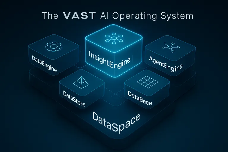
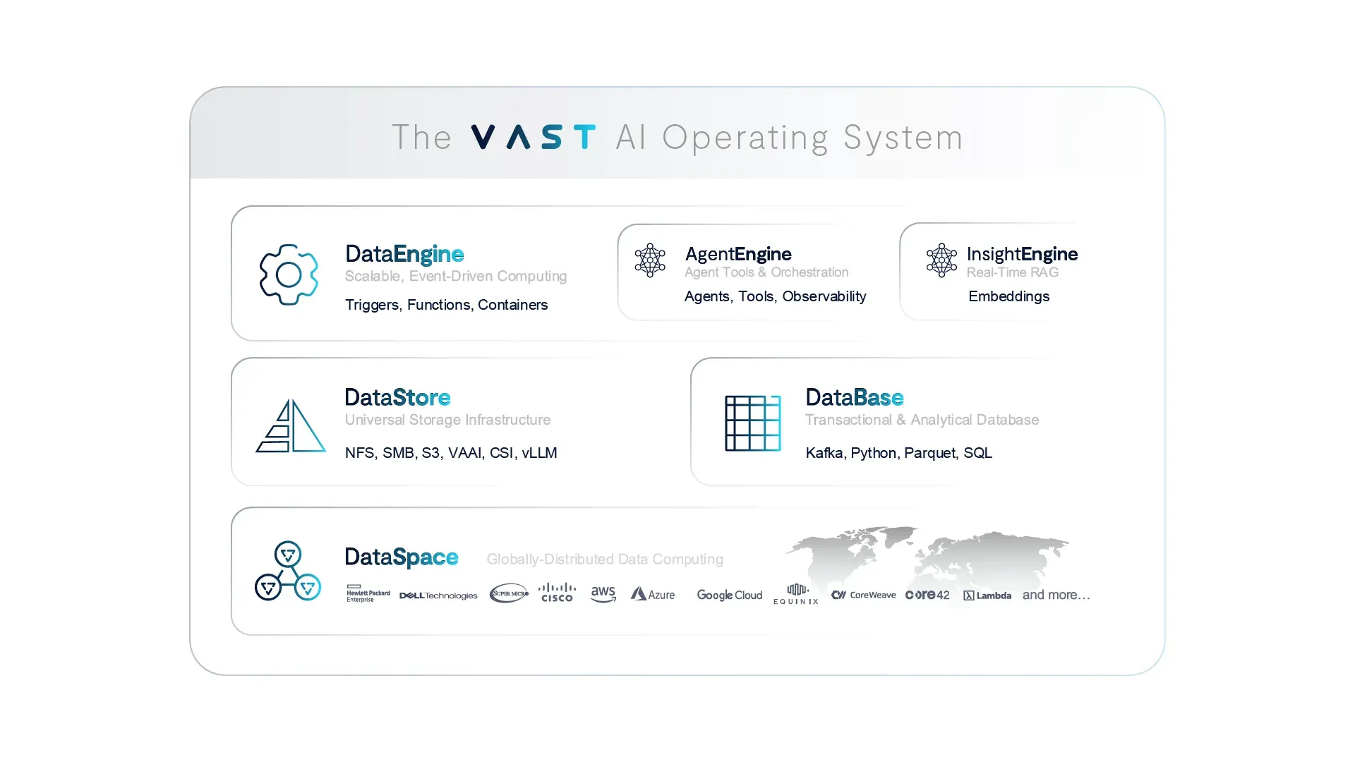
The VAST AI Operating System unifies six key components:
VAST DataSpace: A global namespace for federated compute and storage
VAST DataStore: High-performance storage for unstructured data
VAST DataBase: A real-time, scalable metadata and vector database
VAST DataEngine: A distributed compute engine for orchestrating workloads
VAST InsightEngine: A data refinery that uses AI to generate context and embeddings
VAST AgentEngine: The new AI runtime for intelligent agent orchestration
Together, these components form a cohesive platform designed for real-time data capture, contextualization, and action, making it possible to transition from passive data management to intelligent decision-making systems.
Utility Agents and Developer Enablement
To accelerate adoption, VAST plans to begin releasing a series of open-source utility agents – simple but powerful reference implementations designed to showcase the possibilities of agentic computing. These will include:
A compliance agent to enforce policy and governance
A reasoning chatbot grounded in organizational data
An editor agent for rich media creation
A life sciences researcher for bioinformatics workflows
In addition, VAST Forward, a series of global developer workshops, will provide hands-on training in building on the platform.
The TechArena Take
With this launch, VAST further cements itself as foundational to the next computing era. The AI Operating System is built to democratize access to frontier AI capabilities and make agentic infrastructure a reality for enterprises of every size.
In the words of VAST CEO Renen Hallak, this isn’t just a product launch – it’s the beginning of a new paradigm. And with a clean-sheet architecture, a unified software stack, and support for over a million GPUs already deployed globally, VAST is poised as a leader in the era of the Thinking Machine.

Trump’s Gamble on Global Tech Leadership
President Donald Trump’s recent Middle East tour has marked a decisive pivot in U.S. foreign policy, emphasizing strategic economic partnerships over traditional diplomatic norms. A centerpiece of this approach is a landmark agreement with the United Arab Emirates (UAE) to supply 500,000 of NVIDIA’s most advanced AI chips annually, beginning in 2025. This move signals a significant shift from the previous administration’s restrictive export controls, aiming to bolster U.S. influence in the global AI race.
The proposed deal, nearing finalization, would allow the UAE to import over a million advanced NVIDIA AI chips through 2027. Approximately 20% of these chips would be allocated to G42, a state-backed AI firm in Abu Dhabi, with the remainder distributed among U.S. companies like Microsoft and Oracle establishing data centers in the region. This agreement underscores the UAE’s ambition to become a global AI hub and reflects a broader U.S. strategy to strengthen ties with allies rather than imposing blanket export controls.
However, these efforts raise urgent questions about regional power infrastructure. To activate this scale of AI compute, the UAE has announced plans for up to 5GW of AI data center capacity – equivalent to powering millions of homes. Saudi Arabia’s net-zero AI campus in Oxagon will require an additional 1.5GW of sustained energy. According to the International Energy Agency, global electricity consumption by data centers could nearly double by 2030, surpassing 900 terawatt-hours annually – driven largely by AI demands. Without serious investments in renewables and grid modernization, these ambitions could strain energy systems across the Gulf.
Saudi Arabia’s $600 Billion AI Investment
Simultaneously, Trump secured over $600 billion in commitments from Saudi Arabia, including substantial investments in AI infrastructure. NVIDIA agreed to supply 18,000 of its latest Blackwell GPUs to Humain, a newly established AI firm backed by Saudi Arabia’s sovereign wealth fund. Additionally, AMD announced a $10 billion collaboration with Humain to develop 500 megawatts of AI computing capacity over five years. These initiatives aim to position Saudi Arabia as a leading center for AI development outside the U.S.
This push not only strengthens U.S. alliances, but signals a deeper strategic goal: to redraw the map of global tech power by creating a regional counterweight to China's rapidly expanding AI footprint. According to the Washington Post, the Biden administration had previously warned about unchecked Chinese influence in the Middle East. Now, Trump’s policy appears to take that a step further – arming Gulf nations with the tools to lead their own AI revolutions under an American umbrella.
A New Era of U.S. Export Policy
The Trump administration’s approach marks a departure from previous policies that imposed stringent export controls to limit China’s access to advanced AI technology. By rescinding these restrictions, the U.S. aims to foster innovation and strengthen alliances with trusted partners. However, this shift has raised concerns among U.S. lawmakers about the potential for AI chip smuggling and the need for safeguards to ensure that sensitive technology does not fall into adversarial hands.
Trump’s Middle East strategy reflects a broader vision to counter China’s technological ascent by empowering allies with access to advanced U.S. technology. By facilitating the development of AI infrastructure in the UAE and Saudi Arabia, the U.S. aims to create a counterbalance to China’s growing influence in the region. This approach not only enhances economic ties but also positions the U.S. as a pivotal player in the global AI landscape.
But these moves also raise a deeper question: who will shape the narratives generated by this AI infrastructure? As countries like the UAE and Saudi Arabia invest in national AI platforms, there are rising concerns about the role of AI in information control. In nations where press freedom is limited, there is a risk that state-controlled AI systems could propagate selective or misleading narratives – a form of what some analysts call “AI nationalism.” The ability to generate, curate, and disseminate digital content at scale means these platforms won't just influence global markets – they could influence global truth.
While the long-term implications of these agreements remain to be seen, they undoubtedly mark a significant shift in how the U.S. engages with its allies and addresses global technological challenges.
What’s the TechArena Take?
While President Trump’s approach in the Middle East certainly could strengthen the U.S. position in the AI race, there are inherent risks involved in relaxing export controls, particularly concerning the transfer of sensitive technologies to regional allies. It's also relevant to consider the trend in regional regulatory oversight concerning illicit financial activities. While the UAE has officially condemned terrorism, historical reports have indicated instances where financial networks within the region were implicated in supporting militant groups, including, according to some analyses, in connection with the financing of the September 11 attacks. Therefore, the introduction of such powerful AI technologies necessitates careful consideration of how effectively policies and enforcement mechanisms are evolving to prevent misuse and ensure these advanced tools align with global security norms.
The broader implications of this deal will play out in the coming years, as countries like the UAE and Saudi Arabia evolve into major players in AI, potentially reshaping the geopolitical landscape. For tech companies, this offers a unique opportunity to expand into new markets, but it also calls for vigilance to ensure that technology is not misused or diverted into unintended hands. The question remains: will this strategy ultimately benefit U.S. interests, or will it open the door to unintended consequences that undermine the integrity of American technological leadership – or even the American way of life as we know it today.

Synopsys Accelerates AI Innovation With Microsoft, NVIDIA
In a series of strategic announcements at Microsoft Build in Seattle and NVIDIA's Computex 2025 in Taipei, Synopsys solidified its position as a critical enabler in the rapidly evolving AI and semiconductor landscape.
At Microsoft Build, Synopsys was highlighted as a launch partner for Microsoft's new Microsoft Discovery platform, an initiative aimed at transforming research and development through agentic AI. This collaboration focuses on integrating Synopsys’ AI-driven design solutions with Microsoft's platform to enhance semiconductor engineering processes. Raja Tabet, Synopsys’ SVP of engineering excellence group, emphasized the significance of this partnership, stating that combining Synopsys’ AI capabilities with Microsoft Discovery can “re-engineer chip design workflows, supercharge engineering productivity and accelerate the pace of technology innovation.”
The partnership aims to leverage AI to manage the increasing complexity of chip design, enabling engineering teams to innovate more efficiently. By incorporating agentic AI, the collaboration seeks to create more autonomous and intelligent design processes, ultimately reducing time-to-market for new semiconductor products.

Advancing AI Compute Infrastructure
At Computex 2025, Synopsys announced its participation in NVIDIA's NVLink Fusion ecosystem, a move that underscores its role in advancing AI infrastructure. NVLink Fusion is NVIDIA's initiative to create a semi-custom AI infrastructure by allowing integration of third-party CPUs and AI accelerators with NVIDIA's GPUs. Synopsys’ involvement includes providing silicon design services and solutions that facilitate this integration, enabling the scale-up and scale-out of critical AI infrastructure.
“Data centers are transforming into AI factories,” said Sassine Ghazi, Synopsys president and CEO, highlighting that Synopsys’ solutions are mission-critical enablers in this transformation. By supporting NVLink Fusion, Synopsys contributes to building an open and scalable ecosystem for next-generation AI and high-performance computing.
Enhancing EDA Solutions with NVIDIA's Blackwell Platform
Furthering its collaboration with NVIDIA, Synopsys is integrating its electronic design automation (EDA) solutions with NVIDIA's Blackwell platform. This integration aims to accelerate chip design and manufacturing processes by leveraging NVIDIA's CUDA-X libraries and Blackwell architecture. Synopsys' EDA tools, including PrimeSim, Proteus, S-Litho, Sentaurus Device, and QuantumATK, have demonstrated significant performance improvements when run on the NVIDIA B200 GPU, achieving up to 30x speedups in circuit simulations and substantial gains in other computational tasks.
Sanjay Bali, SVP of strategy and product management at Synopsys, noted that this collaboration “unlocks unprecedented performance gains” and “redefines how EDA is enabling semiconductor manufacturing innovation.” By accelerating simulation and design processes, Synopsys and NVIDIA are enabling faster development cycles and more efficient manufacturing workflows.
Strategic Implications and Industry Impact
Synopsys’ recent collaborations with Microsoft and NVIDIA reflect a strategic alignment with the industry's shift towards AI-driven design and manufacturing. By integrating AI into chip design processes and supporting scalable AI infrastructure, Synopsys is addressing the growing demand for more efficient and intelligent semiconductor solutions.
These partnerships enhance Synopsys’ product offerings and position the company as a central player in the AI and semiconductor ecosystem.
The TechArena Take
The AI boom is no longer about theoretical future states – it’s about practical infrastructure now. What Synopsys has done with Microsoft and NVIDIA demonstrates an important concept: the AI era will be won not only by those building powerful models, but by the companies that empower those models to be designed, validated, and deployed at speed.
Synopsys’ integration with Microsoft Discovery shows how AI will not only be the outcome of innovation but also the engine driving it. By embedding with NVIDIA’s NVLink Fusion and Blackwell platform, Synopsys is asserting its relevance across both the design and deployment layers of the AI stack.
For the industry, the takeaway is clear: if your tools aren’t optimized for AI, you’re already behind. Hats off to Synopsys for helping lead a redefinition of the rules of modern compute infrastructure. This isn’t just EDA innovation; it’s architectural evolution.

Special Report: Data Center Infrastructure Requirements to Scale AI
This special report explores the infrastructure innovations required to support AI-scale data centers, highlighting the escalating demands of generative AI on power, cooling, and rack architecture.
View the Report
Peak:AIO Optimizes AI Infrastructure to Scale Enterprise Adoption
The tech world is evolving rapidly, and few advancements capture attention quite like the transformative shift in AI infrastructure. At the recent GTC conference, one such innovation that stood out was Peak:AIO’s approach to scaling AI technology. We caught up with Scott Shadley, director of leadership narrative and evangelist at Solidigm, and Roger Cummings, CEO and founder of PEAK:AIO, to discuss Peak:AIO’s vision for more intelligent data placement and workload management.
So, what makes this shift significant? Last year, the focus was on simply throwing more hardware at the problem, with rows of GPUs and racks of servers as the go-to solution. However, as we learned from Roger, this approach is evolving. The conversation is no longer about just adding more hardware — it’s about optimizing and refining what’s already in place. This year, the GTC conference revealed a deeper, more solution-oriented approach, where innovation is driven by making the underlying technology not only simpler, but also more efficient for enterprises to adopt and scale.
One of Peak:AIO’s strategies is to focus on maximizing the efficiency of each individual node. By optimizing performance, space and energy efficiency, Peak:AIO is ensuring that each node in an AI infrastructure can deliver six times the performance while maintaining a smaller physical footprint. This efficiency is essential as AI continues to grow more complex and demanding. As Roger aptly pointed out, enterprises can’t afford to let performance bottlenecks slow down innovation, especially as the lifecycle of AI moves from data collection to training and, ultimately, to inference.
This approach doesn’t just apply to large-scale data centers. It’s also vital at the edge, where AI workloads are increasingly being processed closer to the data they need. The role of intelligent storage solutions like those Peak:AIO offers is pivotal in ensuring that data can move efficiently within these distributed environments. By creating dense, high-performance nodes in a 2U frame, Peak:AIO allows businesses to bring AI intelligence closer to the data. This is a game-changer for customers who need the ability to process more data without compromising on speed or efficiency.
One of the most exciting aspects of Peak:AIO’s forward-looking strategy is its focus on AI lifecycle optimization. AI workloads require intelligent data placement and provisioning to ensure that they are always delivered where and when they are needed most. By offering GPU-as-a-service capabilities and prioritizing performance optimization, Peak:AIO is putting businesses in a position to get more out of their existing infrastructure. The result is more cost-effective, efficient and intelligent AI solutions that are scalable as businesses grow and evolve.
So, what the TechArena take? As we look to the future, it’s clear that Peak:AIO is setting the stage for a new era in AI infrastructure. The company’s continued focus on solving performance bottlenecks, optimizing data placement and scaling AI infrastructure is poised to have a lasting impact on how enterprises implement and scale AI technology. For businesses seeking to push the boundaries of AI innovation, Peak:AIO’s solutions offer the intelligent infrastructure required to stay ahead in an increasingly competitive landscape.
For more information about Peak:AIO’s cutting-edge solutions, visit their website at www.peakaio.com or connect with Roger Cummings on LinkedIn. See the related video here.

TechArena Report: 2025 Storage Demands Call for a Change
As AI drives explosive data growth, next-gen SSDs deliver the speed, density, and efficiency to outpace HDDs—reshaping storage strategy for tomorrow’s data-centric data centers.

Databricks to Acquire Neon and Boost AI Agent Capabilities
Databricks, a leading analytics and AI company, announced Wednesday, its agreement to acquire cloud-based database startup Neon in a deal valued at approximately $1 billion.
This acquisition aims to enhance Databricks’ analytics platform with Neon’s serverless open-source PostgresSQL (or “Postgres”) database offering, which provides developers, and now AI agents, with a fast, open and economical option to manage data. We at TechArena noted the purchase with interest, as it is the latest move by Databricks to expand its AI portfolio, following the acquisition of generative AI startup MosaicML in 2023.
Neon, founded in 2021, revolutionized the database industry with an innovative architecture that decouples storage from compute. This technology allows for rapid provisioning, branching, and forking of databases.
These abilities, originally intended to benefit developers, make the solution ideal for AI agents, which require speed and flexibility. In their announcement of the deal with Databricks, Neon revealed that recently more than 80% of databases on their platform were provisioned by AI agents rather than humans.
Ali Ghodsi, co-founder and CEO of Databricks, emphasized the significance of this acquisition: “The era of AI-native, agent-driven applications is reshaping what a database must do. By bringing Neon into Databricks, we're giving developers a serverless Postgres that can keep up with agentic speed, pay-as-you-go economics, and the openness of the Postgres community.”
This move aligns with Databricks’ ongoing strategy to position itself as a top service for building, testing and deploying AI models and agents. It previously acquired MosaicML, an open-source startup specializing in generative AI, with the vision that the acquisition would enable “any company to build, own, and secure best-in-class AI models while maintaining control of their data.” The MosaicML Foundation Series, known for its MPT-7B and MPT-30B models, has enabled organizations to build and train state-of-the-art models using their own data in a cost-effective manner.
What’s the TechArena take? We’ve recently covered how agentic AI is disrupting how enterprises manage their workflows, data, and infrastructure (such as in this Fireside Chat with Intel’s Lynn Comp). Databricks’ acquisition demonstrates how crucial it is for companies to embrace architectures and data management strategies that will prepare them for the increasing demands caused by the accelerated adoption of AI workflows.
We’ll be watching with interest to see how Neon is integrated into Databricks’ offerings, with more information expected to come as part of the Data + AI Summit in June.

Insights on AI and Data Management from Intercontinental Exchange
In today’s rapidly advancing tech landscape, optimizing infrastructure to handle massive data sets has become more crucial than ever. One noteworthy story emerging from NVIDIA GTC is how Intercontinental Exchange (ICE) is tackling the growing complexity of data management, AI implementation and storage optimization across its vast network of financial exchanges, data services and mortgage technologies. We sat down with Anand Pradhan, the head of the AI Center of Excellence at ICE, and Roger Corell, senior director of leadership marketing at Solidigm, to discuss how ICE is using technology to stay ahead of the curve.
ICE, known for operating the New York Stock Exchange, processes over 700 billion transactions daily. With such massive volumes of data, building and maintaining an optimized, highly redundant infrastructure is essential. It’s not just about the network and servers — the flow of data through these systems makes storage a critical focus in ICE’s technology strategy.
Anand explained that ICE handles around 10 to 12 terabytes of data every single day with nanosecond granularity. This data, crucial for tracking financial trades, must be stored and accessed at lightning speeds. With millions of trades, real-time analysis and preventing fraud are key, which means both data retrieval and storage processes must be supercharged for efficiency.
One of the biggest challenges is the sheer volume of data and the input-output bottlenecks that arise when reading and writing to storage systems. To solve this, Anand’s team works closely with the InfraSolutions architecture team to fine-tune the storage infrastructure, ensuring that it scales easily, remains flexible and is resilient to failure. This involves rigorous testing and investment in systems that allow for fast, uninterrupted data access, while minimizing latency and maximizing performance.
But Anand’s insights extend beyond just infrastructure; he also highlighted how AI is shaping the company’s approach to data aggregation. At ICE, AI models are primarily used for processing unstructured data, such as images of real estate properties. The AI extracts valuable insights from these photos, identifying key artifacts, such as doors, kitchens or even the color of a room. With real estate photos pouring in from across the U.S., this AI-driven data processing is a massive undertaking. AI models are deployed at scale to make sense of the raw data, which is then converted into structured, usable information for the company’s real estate services.
As ICE’s AI adoption grows, so too does its need for an optimized storage solution. The storage systems of the future, Anand noted, need to accommodate millions of files — whether flat files, images or video data — and ensure they can be accessed quickly. As more and more workloads move to the AI space, fast access to large datasets and the ability to scale storage seamlessly are becoming essential. This is where storage systems that can horizontally scale, offer fast write speeds and support massive volumes of data will stand out.
Looking ahead, ICE’s evolving use of AI and machine learning is transforming its infrastructure and redefining what modern storage systems must deliver. What’s the TechArena take? With growing demands for speed, scale and real-time access, ICE’s journey offers a clear example of how AI is driving a fundamental shift across the industry. As adoption accelerates, organizations at the forefront of tech will need to rethink their approach to storage — those that do will be best positioned to gain a lasting competitive edge.
To learn more about ICE, visit www.ice.com, or find Anand and ICE on LinkedIn.

What’s next in CVEs Shaping Cybersecurity Compliance in 2025?
The landscape of Common Vulnerabilities and Exposures (CVEs) is evolving in 2025. This shift is driven by the transition of CVE management from MITRE Corporation to the CVE Foundation, and also by increasing recognition of the limits of CVE-centric metrics. By scrutinizing the governance of CVE reporting, one can better understand that more context-aware CVEs are unique identifiers for publicly known information-security vulnerabilities in released software.
For 26 years, MITRE Corporation managed the CVE program, a US government program that identifies and catalogs publicly known vulnerabilities. This centralized effort raised awareness and promoted dialogue on security risks. However, the recent development of the CVE Foundation – spurred by the US government funding uncertainties for MITRE – signals a potential paradigm shift in how CVEs are governed. This transition comes as cybersecurity experts acknowledge, at least privately, that simply counting CVEs often misrepresents their organization’s true security posture. The cybersecurity industry is grappling with the need for more meaningful metrics that genuinely reflect risk reduction, moving beyond performative measures to achieve tangible security improvements.
3 Key Trends Shaping the Future of CVEs & Their Impact on Cybersecurity Compliance in 2025:
1: The Transition to the CVE Foundation: Implications for Governance and Transparency Description: The most significant development is the ongoing transition of the CVE Program's management from MITRE to the newly established CVE Foundation. This shift aims to ensure the long-term sustainability and independence of the program through a more diversified funding model. In April 2025, the US government funding for the CVE program was cut with no transition plan. After public outcry, the US government extended funding for 11 months. This opens the potential for a more globally representative and resilient CVE program, less reliant on a single government funding source. The CVE Foundation (https://www.thecvefoundation.org/) was formed on April 16, 2025 and is actively working toward assuming full operational control and responsibility for the CVE program. Concerns regarding the transparency of its formation, and whether it is sufficiently independent from biased corporate self-reporting, have been raised within the cybersecurity community. This may affect the objectivity and reliability of the CVEs in the future.
2: The Declining Relevance of Simple CVE Counts as a Security Metric Description: There's a growing understanding that merely counting the number of CVEs identified or remediated is a flawed and easily gamed metric for assessing an organization's security risk. Although having an industry-wide quantifiable metric for budgeting, staffing, and tracking progress (KPIs), the severity and exploitability of individual CVEs vary – making simple tallies a poor measure of security improvement. This shift supports a move away from misleading metrics toward more context-aware risk assessments. It also encourages organizations to focus on risk rather than CVE counts. Organizations setting goals to "reduce severe CVEs by 5%" might achieve this by addressing less critical issues, while high-impact vulnerabilities remain unpatched, highlighting the inadequacy of this metric in reflecting true security improvement.
3: The Rise of Context-Rich Vulnerability Assessment and Prioritization Description: The future of cybersecurity compliance is trending toward a greater emphasis on vulnerability assessment approaches that incorporate more context beyond the CVE itself. This includes understanding the specific environment, existing security controls, and the potential impact of exploitation. New market segments, such as Adversarial Exposure Validation, are emerging to provide this richer context. Companies to watch include: Horizon3.ai, BreachLock, Picus Security, Cymulate, and others. These solutions enable m ore effective prioritization of remediation efforts based on actual risk and provide a better understanding of which vulnerabilities pose the most significant threat to a specific organization. Cyber threat actors actively exploit known CVEs – often those for which patches exist but have not been applied. This highlights the need to move beyond counting CVEs to actively validating exposure and prioritizing remediation based on exploitability in a specific environment.
How to Prepare
Organizations should prepare for these shifts by:
- Learning about risk-based vulnerability management: Prioritize remediation efforts based on the severity, exploitability, and potential impact of vulnerabilities within their specific environment, rather than solely on the number of CVEs.
- Staying informed about the CVE Foundation's developments: Monitor the CVE Foundation's announcements and governance structures to understand how the CVE program will evolve and how this might impact compliance.
- Exploring and adopting richer vulnerability assessment methodologies: Investigate and implement tools and services that provide contextual information beyond basic CVE data, such as Adversarial Exposure Validation, to gain a more accurate understanding of their security posture.
- Re-evaluating security metrics: Move away from simplistic CVE counting as a primary security metric and instead focus on measures that genuinely reflect improvements in security and reductions in actual risk.
Conclusion
The landscape of CVEs and their role in cybersecurity compliance is changing in 2025. The transition to the CVE Foundation and the growing recognition of the limitations of CVE-centric metrics signal a move toward a more nuanced and risk-aware approach to vulnerability management. Organizations must adopt better assessment methods to manage risks and stay compliant with their governance frameworks.
- Call-to-action: Share your thoughts on the future of CVEs and their impact on cybersecurity compliance in the comments below. Click here to learn more about risk-based vulnerability management strategies.
- Integration with Automated Security Tools: Discuss how the integration of CVE data with automated security tools, such as Security Information and Event Management (SIEM) systems and vulnerability scanners, can enhance real-time detection and response to threats.
- Machine Learning and Predictive Analytics: Explore how AI is being applied to CVE data to anticipate potential exploits and prioritize vulnerabilities based on historical trends and threat intelligence.
Global Collaboration and Data Sharing: Highlight the role of increased global collaboration and data sharing among cybersecurity entities, including how crowd-sourced vulnerability information and international partnerships could shape the CVE process and improve overall cybersecurity resilience.