
Subscribe to Our Newsletter
Read the latest in the world of AI, data center, and edge innovation.


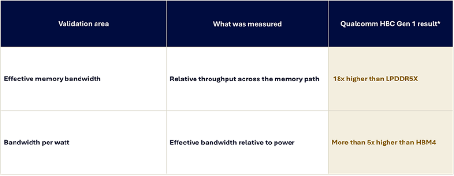
Qualcomm announced Monday that its first-generation High Bandwidth Compute (HBC) silicon has passed validation in the company’s San Diego labs, delivering 18 times the effective memory bandwidth of external Low-Power Double Data Rate 5X (LPDDR5X) and more than five times the bandwidth per watt of High Bandwidth Memory 4 (HBM4) specifications.
The result moves the stacked memory architecture toward commercialization in the Qualcomm Dragonfly AI250 inference accelerator, which is set to begin sampling in the first half of 2027. They also bring an ambition into reality. Qualcomm has argued that memory, not compute, limits AI inference in the agentic era. These results show that HBC is a viable answer to the memory wall, where moving model data between memory and compute consumes much of a system’s time and energy.
As Qualcomm’s SVP & Head of DataCenter Engineering Rashid Attar explained in the announcement and in a recent webinar on TechArena, HBC stacks LPDDR Dynamic Random-Access Memory (DRAM) dies directly on top of an active AI accelerator base die, using wafer-to-wafer direct bonding and through-silicon vias. HBM, by contrast, places DRAM over a base logic die that connects back to a host processor across an ultra-wide memory bus.
Putting compute at the bottom of the stack shortens the distance data travels, which is where much of the energy goes. Because the base die handles the most bandwidth-intensive operations, its link to the main processor needs far less bandwidth.
Engineers drove the silicon on industry-standard automated test equipment through production-representative data paths, using randomized weights and activations at production-representative dimensions. The tester stood in for the accelerator. It set a baseline in LPDDR5X mode, then ran an AI workload in HBC mode and compared execution time and energy.
Source: Qualcomm
Qualcomm described the results as estimates, normalizing measured silicon results to target operating conditions and comparing them with published competitor specifications. The company said redundancy and remapping are built in to work around memory defects, and that it has developed and characterized wafer-to-wafer bonding with foundry and assembly partners across multiple technology generations.
When Qualcomm introduced HBC, it made a specific argument: in the agentic era, inference performance would be won or lost in memory, and moving compute beneath the memory stack was the inside path to victory. Monday’s results put that idea into working silicon. The 18x bandwidth and 5x-plus efficiency gains now rest on a measured chip rather than an architecture slide, and AI250 sampling remains on track for the first half of 2027.
That proof lands at the right moment. Agentic workloads keep long contexts and KV caches resident, which puts memory capacity and bandwidth under constant pressure. An architecture that improves both gives operators a credible path to lower cost per token. Validated silicon shows Qualcomm’s thesis holding up and gives operators a credible path to faster, cheaper agentic inference. The next proof point is AI250 itself, and whether the gains hold at rack scale on real agentic workloads when samples arrive in 2027.
For more on Dragonfly, HBC and Qualcomm’s data center strategy, visit the Qualcomm Dragonfly Media Platform on TechArena.