
.webp)
Subscribe to Our Newsletter
Read the latest in the world of AI, data center, and edge innovation.
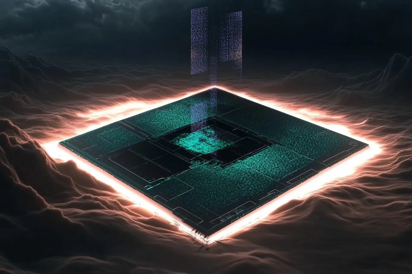
We all know the IT industry is constantly evolving, but now, one of its core technologies is being redefined in the process. I am referring to the processor: the brains of the computer, which are fundamentally being redesigned to change how we build and scale computing systems going forward.
This is happening amidst growing demands for computing power, driven by AI, data analytics, and edge computing. This demand is creating more complexity for design and manufacturing as density, power and integration of functions continue to increase. Traditional silicon scaling of monolithic designs has hit its limits, forcing engineers and companies to explore new ways to achieve performance improvements. Enter: Chiplets!
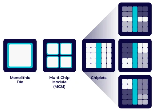
In a nutshell, Chiplets are small, modular silicon dies that function as individual components within a larger processor package. Unlike traditional monolithic CPUs and GPUs, which integrate all processing units and interconnects onto a single silicon die, chiplets are manufactured separately and then assembled into a single package using high-speed interconnects. This approach enhances scalability, improves yields, and enables heterogeneous integration of different technologies within a single processor.
What makes this approach so special is that chiplets allow for the integration of different components (CPU, GPU, memory, network etc.) within a single package. Additionally, chiplets can be fabricated using different manufacturing nodes and processes, optimizing performance, cost, and energy efficiency. This modular design reduces manufacturing complexity, improves yield, accelerates time to market and enhances scalability, addressing key challenges associated with monolithic chip designs.
Chiplets are brimming with potential and are the unsung heroes of innovation, as they bring multiple benefits to the industry.
For decades, Moore’s Law—predicting that the number of transistors on a chip doubles approximately every two years—was the guiding principle driving progress in computing. However, as transistor scaling slows due to complexity, chiplets offer an innovative workaround by allowing manufacturers to integrate smaller, specialized silicon dies into a cohesive system. Chiplets extend the benefits of Moore’s Law without requiring a single, large, monolithic chip. It gets the benefits via a modular approach that enables the use of different manufacturing nodes in a single product, optimizing both cost and performance while reducing production risks.
Allowing different types of processors—such as CPUs, GPUs, and AI accelerators—to coexist within the same package offers a great many benefits. It optimizes performance for diverse workloads, whether in cloud computing, AI processing, or edge devices. By reducing the physical distance between these components, chiplets also cut down on latency and power consumption, enhancing overall system efficiency.
In addition to powering diverse workloads, chiplets also allow manufacturers to create highly customized solutions for specific applications, such as AI, gaming, and high-performance computing. Instead of designing a one-size-fits-all processor, companies can mix and match chiplets to tailor performance for niche markets.
To achieve these benefits, advancements in packaging technologies were required. Innovations such as die stacking—when multiple chips are layered vertically—save space, improve power efficiency, and accelerate data transfer between stacked components. For instance, stacking memory chips directly on top of processors enhances data access speeds while reducing the device’s footprint. Such innovations are reshaping semiconductor manufacturing and delivering more compact, high-performance computing solutions.
In the greater scheme of things, chiplets also make computing systems more energy-efficient and sustainable. For example, the Data Center Multi-Chip Heterogeneous Systems architecture (DC-MHS for short) extends the benefits of chiplet architecture to a system-level. It allows different chiplets to be integrated and upgraded individually, rather than replacing entire chips or servers. This flexibility would theoretically allow you to reconfigure a webserver into a storage or database server by simply swapping out modules, where normally you were confined by the fixed configuration of the motherboard. This modularity extends hardware lifespans, minimizes electronic waste, and optimizes power efficiency.
Evidently, chiplets could herald a turning point for the IT industry, addressing critical challenges in performance, cost, and scalability. As this technology continues to mature, it will redefine everything from data centers to personal devices, making IT infrastructure more powerful, efficient, and sustainable than ever before. Whether in AI, cloud computing, or next-gen gaming, chiplets are shaping the future—one modular building block at a time!